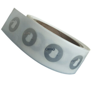
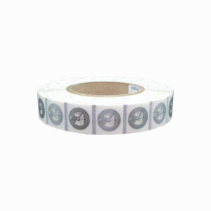
Today, RFID technology has entered all walks of life, playing a powerful digital acquisition capability in different application scenarios and links. However, in practical applications, the identification of labels often encounters a variety of different challenges, including environmental factors, but also including product processes and so on. For manufacturers applying RFID systems, a good RFID tag is a key to the success of the project.
Objectively speaking, a good RFID tag contains many aspects, such as excellent performance, strong storage capacity and environmental adaptability, but also includes a beautiful antenna design, people can not refuse the price and so on.

From the perspective of RFID label manufacturing, the processing methods of each link, including chip, antenna design, binding, composite, and packaging, will have an impact on the final product label. In this process, it is necessary to ensure the performance of the RFID tag and ensure the consistency of the tag. Therefore, even the top RFID tag manufacturers do not guarantee that their labels are “foolproof”.
In the processing of a label, INLAY is usually used as a “sandwich layer” composite material. INLAY enters the composite processing production link as a material, so it must be affected by the five elements of composite personnel, processing equipment, materials, technology and processing environment.
For example, when a customer proposes to attach an RFID tag to a metal, it indicates that he needs a metal-resistant tag. However, this is far from enough, we also need to further understand, what is the material of the pasted metal surface? What kind of dielectric is it? What is the thickness and size of the metal surface? And, what kind of effect the final RFID tag needs to achieve and so on.
In the footwear industry, customers may need large quantities of electronic tags, and will put forward requirements for the surface treatment of electronic tags, and the processor may directly do hot stamping treatment on the surface, or use other processes. In this link, the material used for stamping is also metal. Need to know whether to use cold stamping, or hot stamping process, what kind of dielectric, what kind of material, including hot stamping area and so on.

In the chip processing process, many details will be on the final label. The sensitivity of some chip bindings is very high, and the position and direction of chip bindings are slightly offset, which will have a significant impact on electrical performance. PET aluminum etching antenna will produce volatile gas when heated, in the binding link, heating is to do heating curing, because the conductive glue has been covered on the antenna, may produce bubbles, which will certainly affect the performance.
When we start from the needs, step by step closer to the label processing process, it is more and more close to the essence of a good label, they are composed of countless concrete and small details. As a result, we can also more clearly realize that a good label needs to gather the experience of the entire industry chain, as well as the efforts of countless practitioners.
